Home
Home

 Artists
 Search
 Recent
 Random
 Posts
Posts
 DMs
DMs
 Tags
Tags
 Random
 Importer
 Import
 FAQ
FAQ
 Account
 Register
 Favorites
 Login
Login

Konami 052109 schematic (Patreon)
Content
Confused about those 05xxxx Konami chip numbers yet ? ;3
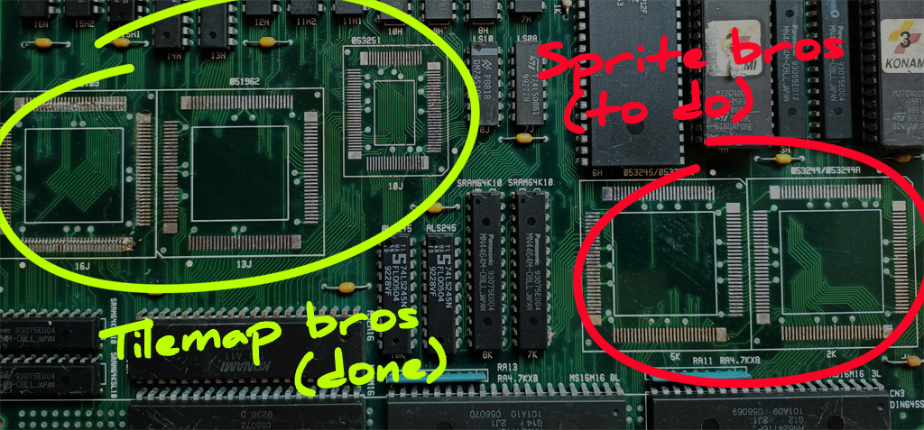
As previously mentionned, this one goes in pair with the last one I worked on: the 051962. They're both used to generate the scrolling tilemap layers (more commonly known as "backgrounds").
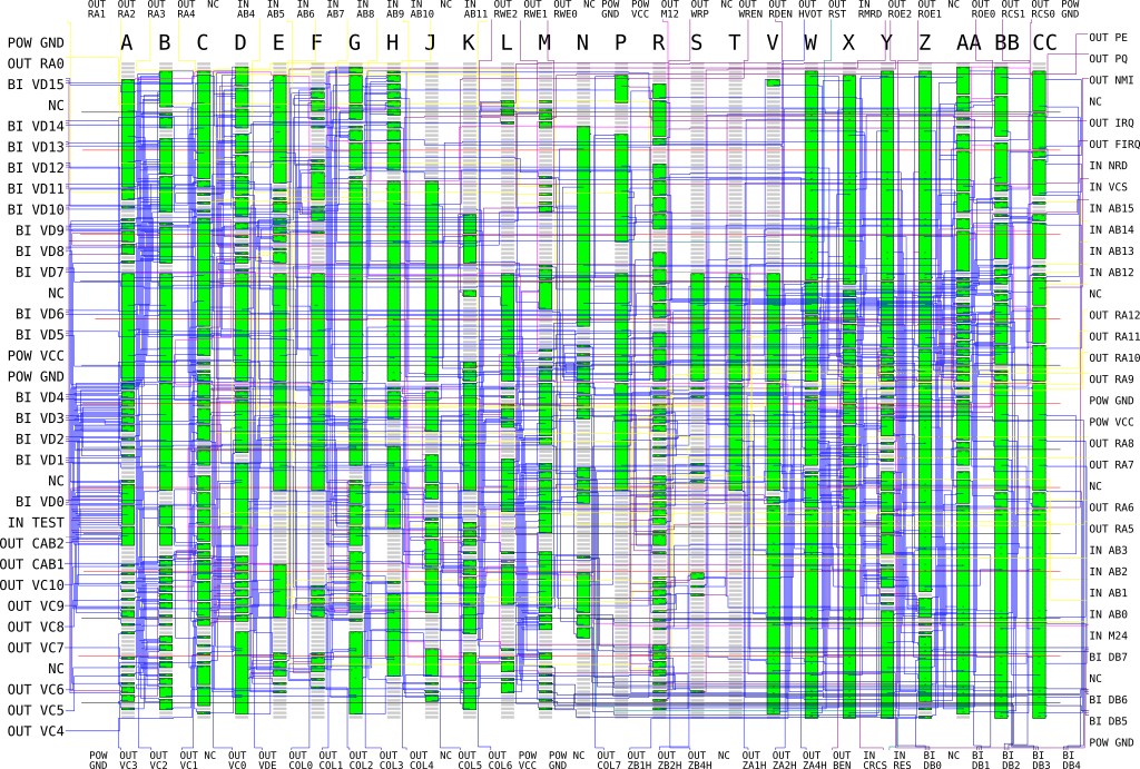
As you can see from the free space (white) on the die trace, the cell usage is noticeably lower than on the 051962. This made tracing a bit quicker, but some previously unseen cells were used, which required careful observation to map their inputs and outputs.
The logic is more complex too: this chip must have enough brains to generate the graphics ROMs addresses from configuration registers, and the contents of the tilemaps in VRAM.
The graphics ROMs are sandwiched between the 052109 and the 051962.
The 052109 tells the ROM which 8-pixel row to get, and the 051962 which pixel to extract. The 051962 then catches the row and grabs the required pixel.
This operation is done sequentially for the 3 layers (A, B, and FIX). Once the 051962 has the 3 pixels ready, it outputs them all at once to the 053251, which then decides which goes on top of the other (priority mixer). This process repeats over and over for each pixel of the final display.
You may be wondering why work with 8-pixel rows before extracting individual pixels ?
This coarse "granularity" is a way to trade bus width against time. The graphics ROMs need some time to be read. Having two 16-bit ROMs in parallel allows one read to give 32 bits worth of data, which in this case equals 8 pixels.
Extracting a single pixel among those is much quicker, so while those 8 pixels are used one after the other, the ROMs have enough time to react to provide the next 8.
This also gives the 052109 enough time to do its thing: for each ROM read, it needs to read the tilemap twice (once for the tile number, once for its attributes), and read the scroll RAM once or twice (X scroll, Y scroll, or both).
The duration of 8 pixels gives it just enough time to collect the necessary data between ROM reads.
The die trace revealed a few not-so-important but interesting things:
- Rather elaborate test logic is present, with one "TEST" pin used as a clock to latch flags that would be presented on the CPU busses. This would be used in factory to check that different parts of the chip are working as expected before being soldered. The pin is then tied low, the test functions never to be used again.
- Significant die space is used solely for the screen flipping option. A register bit is used to flip the whole display around (to accomodate some CRT configurations ?). Several XORs and large adder cells are used to flip coordinates.
- An undocumented register (in MAME) turned out to be used for hardware configuration. Some bits tell the 052109 how many RAM chips are used for VRAM, and what size they are. This is the kind of PCB-level detail that emulation doesn't need to care about.
The schematics and the svg die overlay can be found here: https://github.com/furrtek/VGChips/tree/master/Konami/052109
That's 3/5th of the video chips done. Coming up next are the sprite chips, which work in a similar way (address gen -> graphics ROM -> data demux). This time I'll work on the address generator first.
Files